Lab 4
Lab Goals
The overall goal for this lab is to build a system that can detect treasurers of different shapes and colors. This consists of the following parts:
- Arduino-Camera communication
- Arduino-FPGA communication
- Camera-FPGA communication
- Color detection with the FPGA, Camera, and Arduino
Prelab Questions
- From the FPGA’s specifications, what is the maximum size of the buffer you can create? Given that each entry is ___, how many entries large can the RAM be?
- Total RAM = 594 Kbits = 74250 bytes
- The OV7670 offers a variety of pixels formats to sample data. Which of the formats available provides the most info on the base colors making up each pixel?
- Image sensor can output the following:
- QCIF 176 x 144 = 24768 bytes can fit
- YUV/YCbCr 4:2:2
- RGB565/555
- GRB 4:2:2
- Raw RGB Data
- Use RGB565 since it maintains the most information
- Given that the input to the VGA adapter is RGB332, how can you convert (downsize) the pixel format from Q2 to be accepted by the VGA module?
- Starting with the RGB565 pixel format, take the most significant bits to downsample to the VGA-accepted RGB332 format
- Now that you know the downsized memory per pixel (from Q3), you need to know how many you can fit into memory. Which of the predefined resolutions that the OV7670 supports provides the max amount of pixels in an image, given the constrained max size of the buffer (from Q1)? What’s the size of the buffer?
- QCIF 176 x 144 = 24768 bytes can fit
- Using the Register Set table on pages 10-23 of the OV7670 datasheet, find the registers you will need to set.
- Please see the Arduino section below
- Take a look at the timing diagrams (Fig 5 and 6) on Page 7 (Ignore HSYNC, you won’t use it). Use both diagrams to determine when you should sample your data. (Hint: You only want to sample valid bytes, and each one only once)
- HREF signal is high during readout of a single row, and low in between readouts of rows
- VSYNC is set high after all rows of a single frame have been read out, signaling the start of a new frame
- RGB565 uses 16 bits to represent a single pixel, so requires two cycles to output since the camera outputs 8 bits in parallel per cycle
- Data is fully valid every other cycle when HREF is asserted
- Timing diagrams shown below in Downsampler portion of the FPGA section
- Discuss with your entire team, what method you want to use to communicate information from the FPGA to the Arduino. Parallel? Serial?
- For this lab, we are going to use parallel communication
- We have open pins on the Arduino we are using
- Easy to implement
- For the actual implementation on the robot, we are going to use software-serial
- We have a pin-shortage
Sub-Teams
To begin, we split into two groups of two. Each group progressed through the lab individually, as described below.
- Arduino & Camera Team = Kenneth and Tyler
- FPGA Team = Brian and Eric
Arduino & Camera Team
GOAL: setup the camera and create an FPGA-Arduino communication protocol
Materials Used
- 1 × Arduino Uno
- 1 × OV7670 CMOS Image Sensor
- 1 × 3V Regulator
- 2 × 10 kΩ Resistors
- 2 × 4.7 μF Polarized Capacitors
- 1 × mini-breadboard
Wiring Arduino-to-Camera
- First, we DISABLED INTERNAL PULL-UPS ON ARDUINO
- Tyler discovered how to do this on Mac (see Piazza post)
- Without this, the I2C signals would be pulled up to 5V, which would break the camera
- We wired a 5V input from the Arduino to a 3.3V regulator, with capacitors on the 5V input and 3.3V output to stabilize the power supply
- NOTE - the regulator’s output will not be 3.3V unless it is loaded
- For testing our regulator we added a 330 Ω resistor and measured the output pin
- We wired up the schematic provided in the lab, which sets up I2C communication with the camera for programming
- NOTE - pin names on the camera differ from the diagram below
- SIOC = SCL
- SIOD = SDA
- MCLK = XCLK
Credit to Kirstin for both schematic diagrams
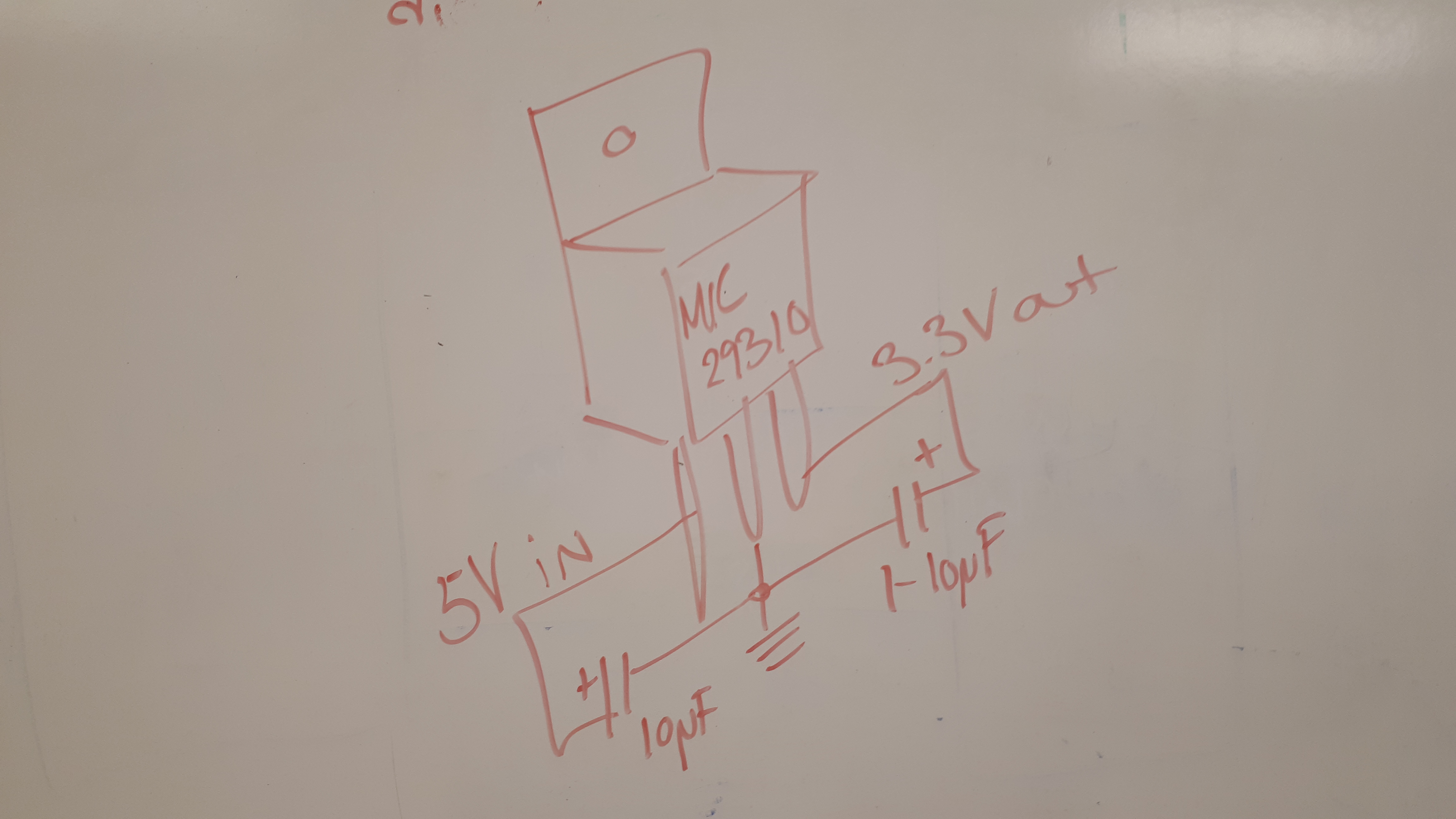
Camera-to-Arduino power schematic
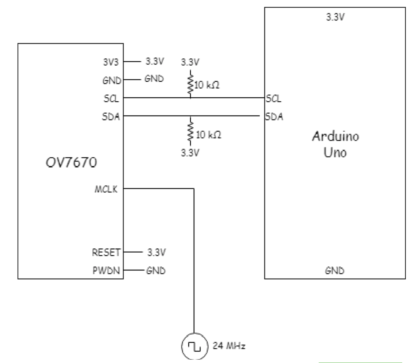
Camera-to-Arduino I2C schematic
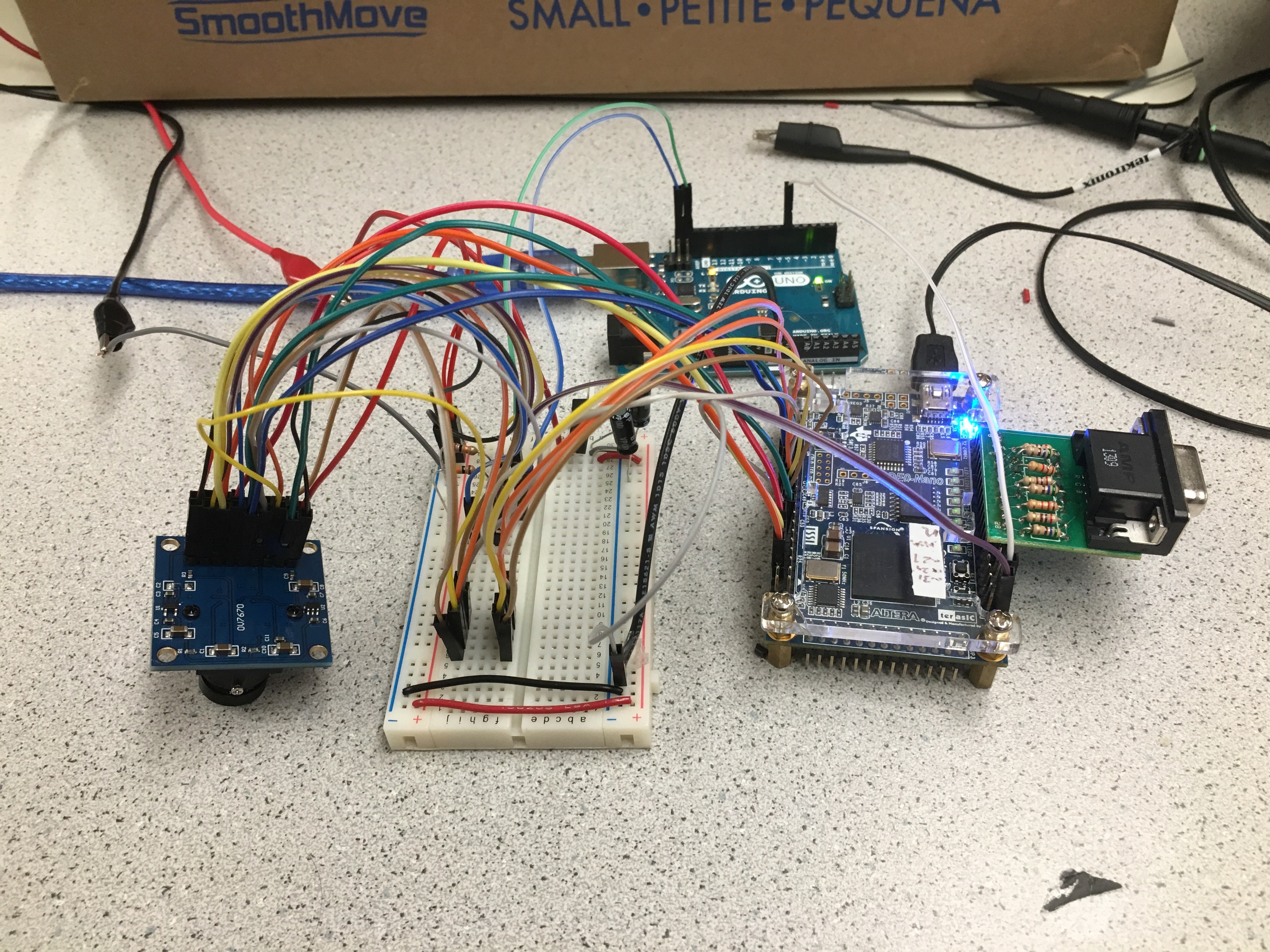
Full system wiring
Programming the Camera
- The camera has control registers defined by their Serial Camera Control Bus (SCCB) interface
- We can use this interface via I2C from the Arduino
- Here are the control bits we need to set, and in which register (the format is REGISTER_NAME[bit_index], bits are 0-indexed):
- COM7[7] = 1
- COM7[3] = 1
- COM7[2],[0] = 1, 1
- COM7[1] = 1
- COM3[3] = 1
- COM9[6:4] = 000
- COM9[0] = 1
- COM15[7:6] = 11
- COM15[5:4] = 01
- COM17[3] = 1
- CLKRC[7] = 1
- CLKRC[6] = 1
- MVFP[5] = 1
- MVFP[4] = 1
- The camera I2C slave addresses are found on page 10 of the camera datasheet
- 0x42 = write address
- 0x43 = read address
- NOTE - Arduino’s Wire library fills in the LSB based on whether we are reading or writing
- The actual address we use when calling the Wire library is 0x21 (the 7 MSB of the above slave addresses
- NOTE - all values will be read in hexadecimal format
- All addresses and write values should also be written in hex
- Be sure you specify that format in your code (eg. 0xAB)
- We used the provided read_register_value() function to create a function read_key_registers()
- We use this as a diagnostic tool to print out the values in all of the target registers
- It is the first function called, and then is called again after writing to the registers
- This allows us to compare the results to make sure we set the correct registers to the desired value
← Output format - QCIF selection
← Output format - RGB selection
← Color bar enable
← Scale enable
← Automatic Gain Ceiling (2x)
← Freeze AGC/AEC
← Data format - output full range enable
← RGB 565 enable
← DSP color bar enable
← Enable digital PLL option
← Use external clock directly
← Mirror image enable
← VFlip enable
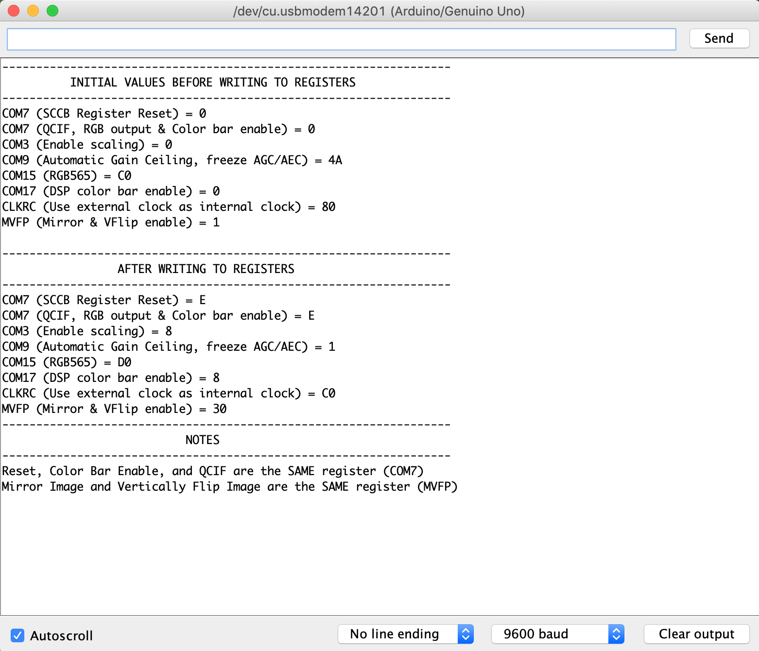
Setting up the camera registers
Creating FPGA-to-Camera Communication Scheme
- For the competition, we need to be able to detect the following:
- Presence of a treasure
- Color detection - blue or red
- Shape detection - triangle, square, or circle
- We created the below table to encode this information into 1 byte
- Although we are using a full byte, the 7 possibilities fit into just 3 bits
- In Lab 4, we only need to be able to detect color: Red or Blue
- This is easily done with one wire from a GPIO pin on the FPGA to a digital I/O pin on the Arduino
- During the competition, when we need to transmit three bits at a time, we plan to use software serial
- This is more challenging to setup
- Only requires two pins -> we only have two pins available
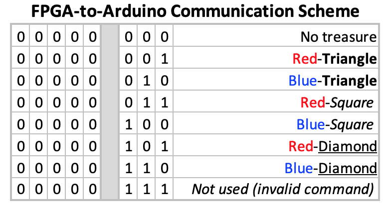
FPGA-to-Arduino communication scheme
FPGA Team
GOAL: setup the FPGA to perform shape and color detection
Materials Used
- 1 × DE0-Nano Development and Education Board
- 1 × GPIO-to-VGA adapter
- Altera Quartus Software
PLL and Clocks
- Created a Phase-Locked Loop (PLL)
- Takes a 50 MHz clock input
- Outputs 24 MHz, 25 MHz, and 50 MHz clocks
- The 24 MHz clock is used to drive the camera
- The 25 MHz clock is used for the downsampler, image processor, and VGA driver
Buffer Reader
- Display test pattern across the VGA Driver by writing a test array to memory and reading from it
- Update the X_ADDR and Y_ADDR, since these form the write address in memory corresponding to the pixel that is to be displayed
- If X_ADDR < 50, write a green pixel
- Else if X_ADDR < 80, write a blue pixel
- Else write a red pixel
- Once this is written to memory, VGA driver continuously reads all the pixel values in memory and displays them
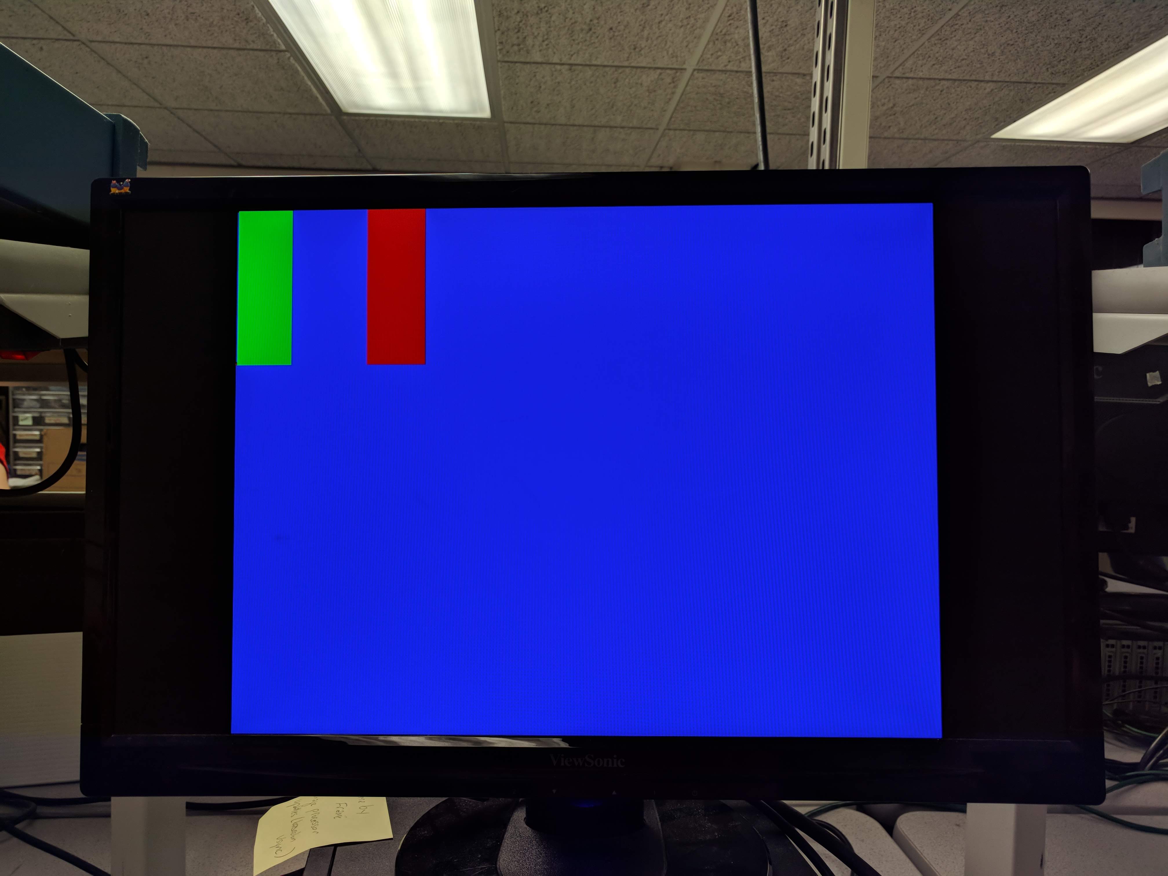
Buffer reader test image
Downsampler
- The camera is set up to output RGB565 pixel format, thus there are:
- 5 bits for the red channel
- 6 bits for the green channel
- 5 buts for the blue channel
- A total of 16 bits per image
- Since the camera outputs 8 bits in parallel at a time per pixel, 2 clock cycles are needed to output all 16 bits that represent a single pixel
- The output is broken up as follows:
- Byte on first cycle = 5 bits of red + 3 bits of green
- Byte on second cycle = 3 bits of green + 5 bits of blue
- See the RGB565 timing diagram below for more information
- To downsample to RGB332, simply take the 3 MSB’s of red, 3 MSB’s of green, and 2 MSB’s of blue
- HREF signal is asserted during a readout of an entire row of pixels, and is low in between row readouts
- After all rows have been readout in a single frame, VSYNC is asserted
- See the VGA frame timing diagram below for more information
- Every two cycles of PCLK (clock at which pixels are readout from camera):
- a valid RGB332 pixel value is produced
- W_EN needs to be asserted
- In top level, use readout sequence with HREF and VSYNC to determine the address in memory that needs to be written to during readout and when it is to be incremented
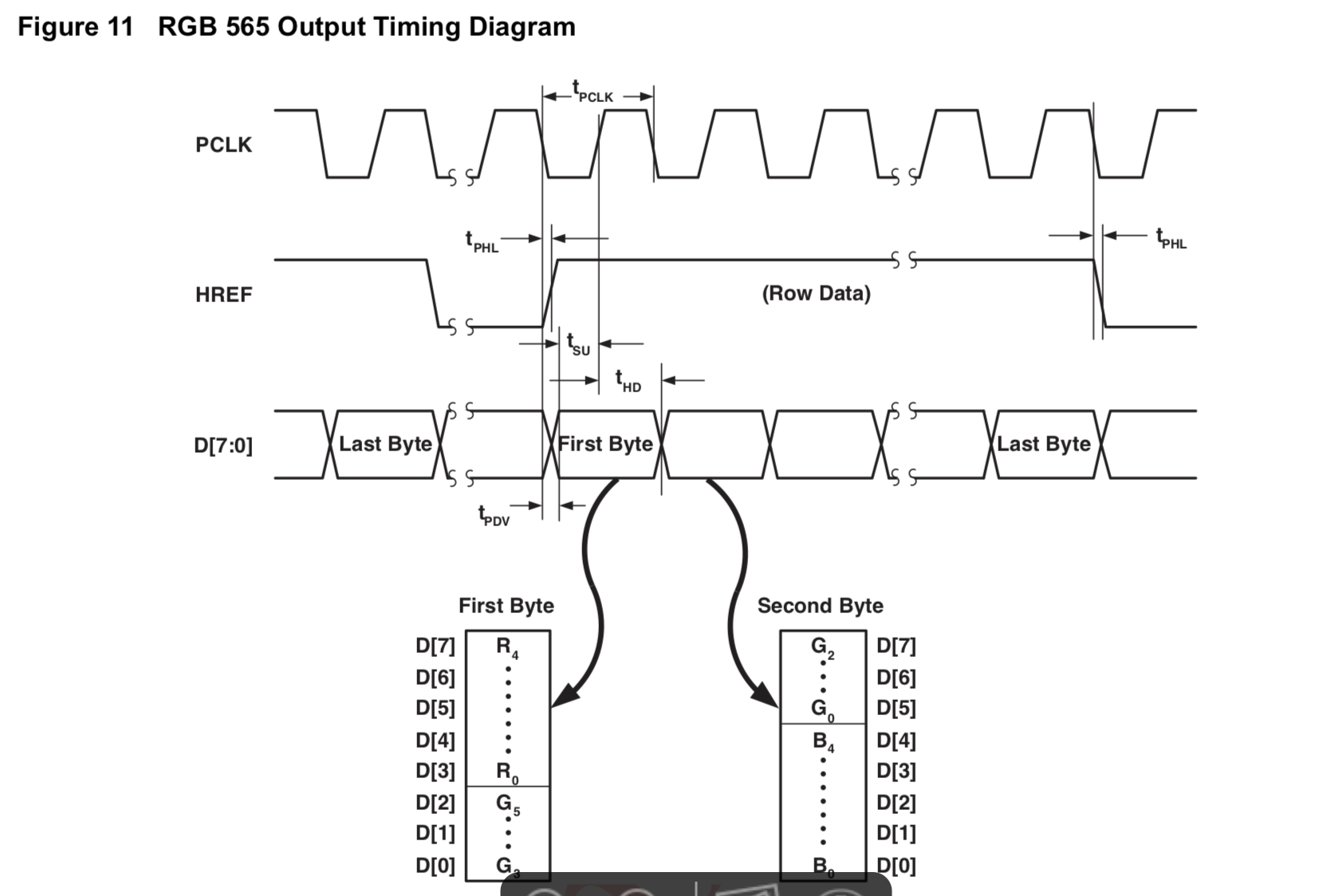
RGB565 timing diagram
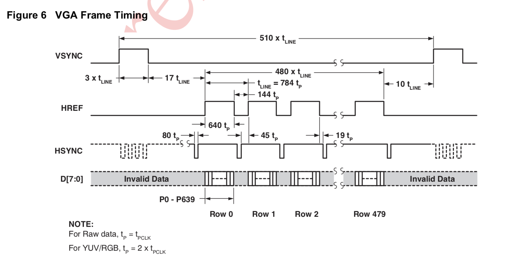
VGA frame timing diagram
Color Detection
- For this lab, the color detection task consisted of determining whether a given image was primarily blue or primarily red
- Determine this by counting frequency of pixels with an R value > B value
- Every VGA clock cycle, the image processing block reads a new pixel from memory
- The downsampler stores three bits of red information and two bits of blue information
- Given this, we count the number of times the two most significant bits of red are greater than the two most significant bits of blue
- If this counter exceeds half the number of pixels in the image (12672) by the end of the frame, the image was majority red
- Every time VSYNC rises to signal a new frame, we update an output pin according to:
- Majority red = HIGH
- Majority blue = LOW
Full System Testing
This video demonstration shows our robot completing all required behaviors:
- Uses the camera to capture a live image
- Downsamples that image from RGB565 to RGB332 on the FPGA
- Displays that image on the monitor through the VGA adapter
- The FPGA processes the data to determine if the image is red or blue
- The FPGA transmits that information to the Arduino
- The Arduino prints the results onto the Serial monitor